Novel high-conductivity 2D semiconductors identified in new research
by Carey Sargent, NCCR MARVEL, EPFL
Two-dimensional (2D) semiconductors with excellent intrinsic transport properties could be a boon to transistors and used in a range of applications such as opto-electronic devices. Though some well-known 2D materials like transition-metal dichalcogenides, phosphorene or silicene have already been studied extensively and other candidates for extensive investigation have been identified, it’s likely that many additional promising materials exist.
Indeed, in an earlier paper, “Two-dimensional materials from high-throughput computational exfoliation of experimentally known compounds,” the authors identified more than 1,000 materials that can be easily exfoliated from their parent compounds and others can be synthesized.
Though finding the ideal material for a given device would require cross-examination and the co-optimization of many different properties, identifying the physical features that lead to good transport performance is a solid basis for further investigation. In the paper Profiling novel high-conductivity 2D semiconductors, recently published in the journal 2D Materials, researchers described the tools and knowledge needed to explore large databases with an informed, purposeful approach. Focusing on phonon-limited conductivities, and studying 2D semiconductors doped by field effects, they used the technique to identify candidates with the highest conductivity.
Restricting their selection to no more than 6 atoms per unit cell to limit computational cost, the scientists first used a band structure analysis to select the most promising materials from a Materials Cloud database of 2D materials they had already found to be exfoliable from experimentally known 3D compounds. They then studied the transport properties of the materials using an accurate, automated framework they recently developed. This approach featured two main advantages compared to other methods in the context of their study. On the one hand it included several tools to analyze band structure properties like valley structure or Fermi velocity. On the other, the calculation of conductivity is automated within the AiiDA framework and this is a critical feature for being able to study many materials in high-throughput fashion. The tools used are available in the Archive section of the Materials Cloud, in support of the FAIR principles of open science and open data.
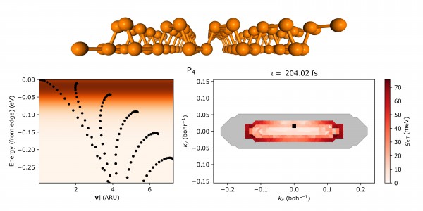
The researchers, Thibault Sohier, Marco Gibertini and Nicola Marzari, first analyzed electron-phonon scattering in two well-known high conductivity 2D semiconductors systems—electron-doped InSe and hole-doped phosphorene—to identify representative band features. Though both are single-valley systems with weak electron-phonon interactions, they represent two distinct pathways to fast transport: the former has a steep and deep isotropic valley, while the latter features strongly anisotropic electron-phonon physics.
Having identified the representative features, they then searched for features in the Materials Cloud database and computed the transport properties of the most promising candidates. The selection process relied solely on band properties (gap, valley positions, velocities) and all 256 easily exfoliable, dynamically stable and small unit-cell materials were considered. Electron-phonon scattering was analyzed in each monolayer. The approach allowed them to find several promising 2D semiconductors.
They found excellent phonon-limited transport properties in electron-doped Bi2SeTe2, Bi2Se3, BiClTe, Sb2SeTe2, InSe, GaSe, AlLiTe2 and hole-doped phosphorene (P4), AuI, ClGaTe, and WSe2, all with mobilities in the range from few hundreds to few thousands cm2/Vs. Three of the materials are very well-known and studied (P4, WSe2, InSe), and, while the Sb2X3 and Bi2X3 (X = Se, Te, S) compound monolayers have been recently investigated in the context of phonon-limited transport, they are better known for the topological properties of their 3D parents. The transport performance of monolayer Sb2SeTe2 has been confirmed experimentally. GaSe (along with InSe) was studied ab initio with a representation of electron-phonon scattering that goes beyond deformation potential theory while their research was being carried out. AlLiTe2, BiClTe, ClGaTe, and AuI are, to the knowledge of the authors, still new in the context of 2D charge transport.
Beyond the relatively large number of materials identified and the novelty of some of them, the paper gave visual and intuitive understanding of electron-phonon scattering as well as a systematic and data-supported analysis of the features leading to good transport performance.
The researchers confirmed the importance of band properties such as number of valleys, effective masses or anisotropy and showed that they can be used to shortlist prospective conductors in larger scale databases. Comparing the 11 monolayers in detail also allowed them however to observe how the strength and angular dependency of electron-phonon scattering drives key differences in the transport performance of materials despite similar valley structure. The high conductivity of hole-doped WSe2 also revealed the limitations of any selection process based on band properties alone.
Reference:
T. Sohier, M. Gibertini, and N. Marzari, Profiling novel high-conductivity 2D semiconductors, 2D Materials 8, 015025 (2020). [Open Access URL] / Dataset on Materials Cloud
Low-volume newsletters, targeted to the scientific and industrial communities.
Subscribe to our newsletter